Watch out for WannaCry

Recently, the world’s largest manufacturer of semiconductor chips, Taiwan Semiconductor Manufacturing Co. Ltd. (TSMC), was hit with the WannaCry worm. A supplier installed software containing the infection to a tool and connected it to the network. More than 10,000 unpatched Windows 7 machines became infected, leading to substantial losses in production while machines were down as a result of the worm and the subsequent efforts to repair the damage.

Installing the patches themselves requires taking the machines down and coordinating tool recovery with equipment suppliers.
You can read more about the event here.

As more and more systems in manufacturing facilities are networked together, the threat of worms like WannaCry increases. Managers need to trade off the improved productivity of networked systems against the downtime needed to properly secure those systems against viruses and worms, also considering the threat of greater downtimes from an infection.

Most of the NanoScope® brand AFM’s are controlled by Windows XP computers. Accordingly, the computers supplied by Advanced Surface Microscopy for refurbished systems run Windows XP to retain compatibility with older hardware. Systems installed after May 2017 have the XP WannaCry patch that was provided by Microsoft.


If you have an XP system, here’s how to confirm the patch is installed:

  • Open Windows Explorer and browse to the indicated folder and file.
  • Highlight the file srv.sys and read the file version in the status line.

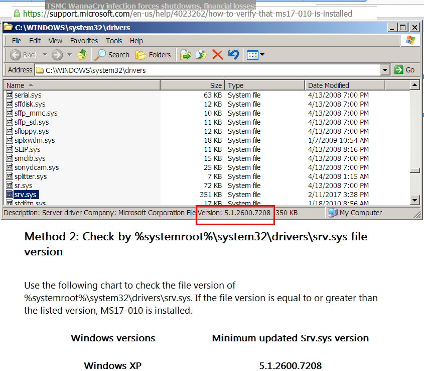
  • Srv.sys version 5.1.2600.7208 is good. If you have this version, the patch is installed.
  • Then close the Window.

If the patch has not yet been installed, then:

Download and install the patch Security Update for Windows XP SP3 (KB4012598).
You can find this at https://www.microsoft.com/en-us/download/details.aspx?id=55245
The file to download is
WindowsXP-KB4012598-x86-Custom-ENU.exe
Date Published: 5/15/2017
File Size: 666 KB

For all other operating systems, go to the authoritative Microsoft page.

ASM Buys and Sells Used (Second-Hand) NanoScope AFMs

This page contains [will contain] links to several pages describing used (second-hand) NanoScope equipment we have for sale and seek to buy.

ASM buys, refurbishes, and sells and installs used AFM and STM equipment.  The equipment shown on these pages is representative of what he have bought and sold in the past.  Similar systems are generally available, but current stock may not match the exact configurations shown here.

Ask us for details of currently available systems.

Would you rather fix what you have then buy?  We also repair NanoScopes.

Equipment we Sell

Equipment we buy

Reference Information

Why Buy from ASM

Since 1990 we have bene providing skilled analytical services specializing in Atomic Force Microscopy and related techniques.  We have made significatn scientific contributions in AFM.  Since 1993, we have been buying, refurbishing and selling, second-hand NanoScope AFM’s and related equipment for customers around the world.  All the equipment we sell is tested and repaired as needed to meet our professional standards.  We provide skilled techinical support to our customers, covering both instrument operations and application advice.

What Customers Say

“I thought the AFM purchased by Molecular Reflections was an excellent instrument.  No surprises.  I also think that you and your colleagues wanted us to succeed, not only in getting the instrument functioning but beyond, in terms of guidance for techniques and such.  I would highly recommend Advanced Surface Microscopy as a source for renewed equipment.” – Dr. Boyce Collins, USA.

“I always thought it was a great idea to have a company that sells used SPM equiment.  Advanced Surface Microscopy provides an excellent service to the SPM community with its products.” Prof. Ricardo Garcia, CSIC-Madrid Microelectronics Institute, Spain.

Analytical Services

  • Topographic Height Imaging
  • Additional Image Modes
    • Phase Imaging:  Done in tapping mode, phase imaging allows mapping of material domains on the surface.  Phase images are sensitive to stiffness and adhesion (stickiness) of the surface as well as edges and boundaries.  Phase images can provide important information on a variety of characteristics of the sample at the micron to nanometer scale.
      • Material Distributions and Chemical Domains in Polymer Blends and Copolymers
      • Presence of Contaminants
      • Inhomogeneity of the Sample surface
    • Lateral Force/Friction Imaging:  Done in contact mode, friction imaging measures the twist of the probe as it is scanned across the surface.  this twist corresponds to the sideways force on the tip from factors like surface slope and coefficients of friction between the surface and the tip.
    • Force Volume Imaging:  While being scanned over the surface, the tip is pressed into the surface at each point and the response of the tip measured.  Allows mapping of surface stiffness and adhesion.
    • Techniques Involving Long Range Forces:
      • Lift Mode for Measuring Long Range Forces:  Most electrical and magnetic force work is done using “Lift Mode.” The tip first scans each like of the surface, then repeats the motion over that line, following the trace a preset distance above the surface.  During this second trace, the response of the tip to long-range forces such as magnetic or electrical forces is measured and an image is generated based on these measurements.
      • MFM:  In this a magnetized or magnetically sensitive tip is used for the lift mode image.  The tip reacts to magnetic forces near the sample allowing mapping of magnetic domains on the nanometer scale.
      • Electrical Techniques Involving Long Range Forces:
        • EFM:  Similar to MFM but an electrical charge is applied to the tip.  The tip then reacts to electric fields near the surface and allows them to be mapped on the nanometer scale.
        • Scanning Kelvin/Surface Potential Imaging:  Maps the wok function or surface potential of the surface.  This technique is sensitive to many surface phenomena.  Some characteristics that can be mapped include catalytic activity, doping and band-bending of semiconductors, charge trapping in dielectrics, and electrochemical differences such as those involved in many kinds of corrosion.
    • Electrical Measurements in Contact with Surface
      • Scanning Capacitance Microscopy (SCM):  A powerful tool in studying seminconductor samples.  Scanning Capacitance Microscopy allows direct measurement of activated carrier concentration on non-uniformly doped semicondutors with nanometer scale accuracy.
      • Scanning Spreading Resistance Microscopy (SSRM):  Another powerful tool for studying semiconductors and conductive polymers.  SSRM allows mapping both topography and dopants on the surface of conductive samples.
      • Conductive AFM (CAFM):  Maps variations in electrical conductivity.  Can be used to do things like study semiconductors, Nanotubes, Conductive Polymers, and even certain organic materials.
      • Tunneling Atomic Force Microscopy (TUNA):  Similar to CAFM but with much higher current sensitivity (<1 pA).  Can measure conductivity through thin films and work with low conductivity samples.
    • Nanoindentation and Scratching:  Measure and test hardness, wear resistance on the Micro and Nano scale.  The AFM presses a diamond tip into the sample surface and either withdraws, leaving an indent, or drags the tip across the surface leaving a scratch.  The AFM then produces an image of the resulting indent or scratch.
    • Tribology on the Nanometer Scale:  The combined use of height and friction imaging, roughness measurement, and Nano-scratching and indenting allows studying the tribology of materials on the nanometer and micrometer scales.


  •  And these processes can be used to treat the results of numerous processes including:
    • Cleaning
    • Coating
    • Corrosion
    • Cracking
    • Etching
    • Extrusion
    • Microlithography
    • Molding
    • Nanolithography
    • Optical Disk Mastering
      • Track Pitch Measurements on optical discs (CD, DVD, HD-DVD, Blu-Ray, etc.)
      • Feature Size, Shape, and Position Measurements in Optical Disks
    • Optical Disk Replication
    • Optical Grating Fabrication
    • Plating
    • Polishing
    • Polymerization
    • Purification
    • Rolling
    • Texturizing