AFM For Energy Technologies
Atomic Force Microscopy has many uses in energy technologies.
Semiconductors
Whether it’s photovoltaic cells for solar power or control circuits for coal power plants. Atomic Force Microscopy provides an in-depth look at the surface structures of electronic materials such as semiconductor wafers.

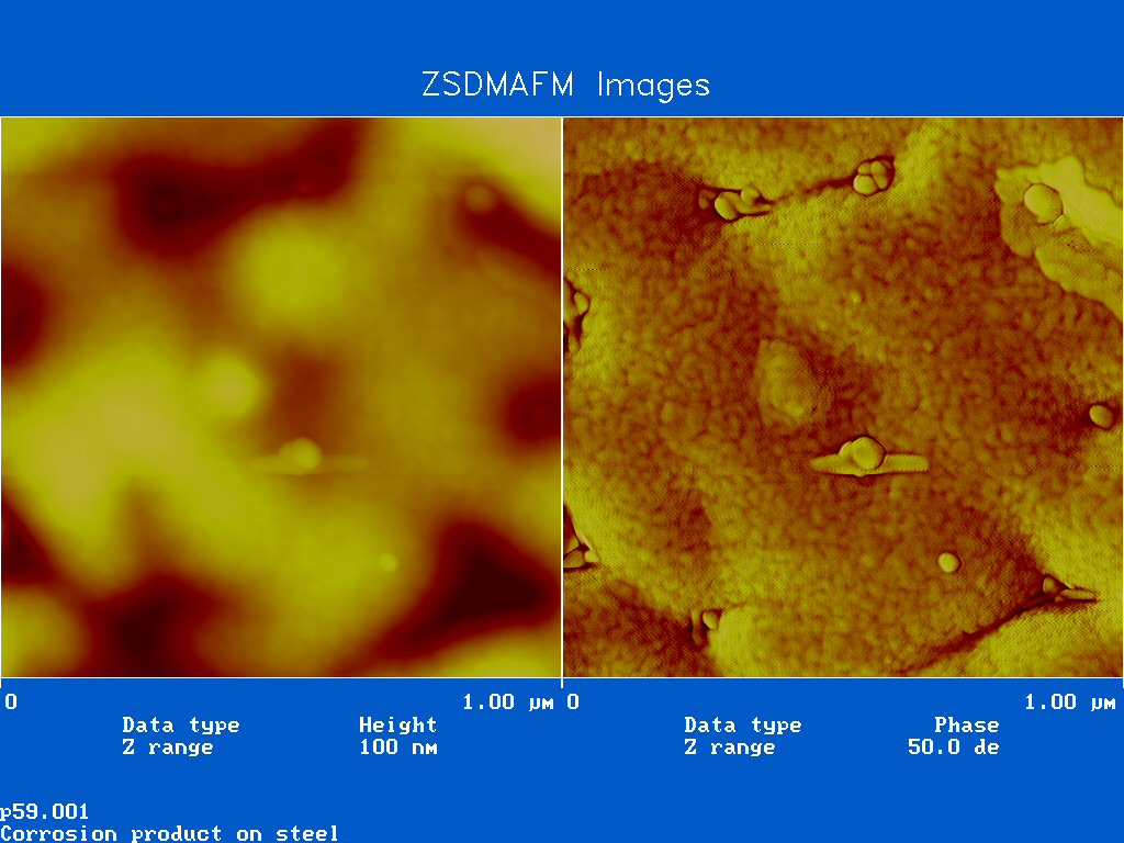
Corrosion
Materials used in energy production are often exposed to harsh and corrosive environments. The ability of AFM to reveal the microstructure of the surface, showing the initiation and progress of materials after exposure to these environments helps engineers understand the corrosion process and find better ways to fight it.
Catalysts
Whether it’s manufacturing of materials, encouraging chemical reactions for power production, or reduction of harmful emissions, catalysts play an important roll in energy technologies. In addition to the catalysts’ chemical compositions, their physical structure, particularly at the surface, is vital to high performance. Atomic Force Microscopy allows engineers to delve into that structure in in detail.
New Materials Including High-Strength Magnets
New challenges in the energy field call for new materials to meet them. Whether it’s advanced composites for wind turbines, superalloys for high temperature applications, or powerful magnets for high efficiency motors and generators, understanding the microstructure of these materials is key to improving their performance. Atomic Force Microscopy provides three dimensional maps that reveal that microstructure in ways no other technique can. In addition, AFM can map long range forces like magnetic and electric fields providing a better understanding of these properties in new materials.