The Scanning Tunneling and Atomic Force Microscopes are well-known due to their extraordinary capability of imaging atoms using a simple mechanism.
highly ordered pyrolitic graphite (HOPG).
However, atomic resolution is usually not needed to solve most problems in development and manufacturing. As a result, many scientists mistakenly regard these new microscopes as more exotic than practical.
Both the AFM and STM make 3-Dimensional images of solid surfaces, but the AFM has much broader applications. The reason for this is that the AFM uses a universal sensing mechanism (repulsive and attractive mechanical forces), whereas the STM uses an electrical signal, which requires that the surface be at least somewhat conductive.
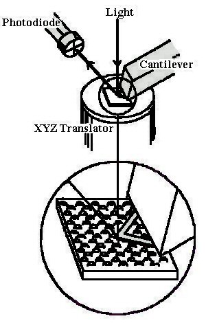
scanned over the surface, the cantilever
deflects upward, changing the angle
of the beam of light reflected to the
split photodiode. This allows the tip
to accurately track the surface.
Using the extraordinary height sensitivity and wide scan capabiity of the AFM, we can easily answer simple but important questions about surfaces and surface features including:
- Is a contaminant present
- Is a feature a pit or a peak
- How tall is it
- What is the grain size of a coating
- How rough is the surface
- Is a coating continuous or broken
Answering these questions and others like them provides several applications which have practical value for a diverse group of industries. We provide several examples.
AFM Image of Aluminum Foil
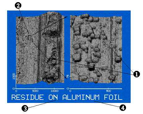
AFM images of aluminum foil show many shallow bumps (5-25 nm high), which cover features associated with the rolling process (such as large tears and fine scratches). It is evident that the bumps are depositied after the foil emerges from the rollers. We believe this contaminant is a non-volatile residue derived from the rolling lubricant. The ability to detect the amount of residue on the foil surface helps metallurgists improve product clenliness.
Magnetic Recording Heads
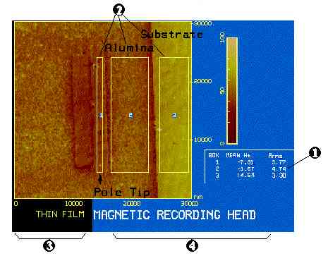
showing height difference between different
elements of the head.
High Density Magnetic Storage depends on precise fabrication of the recording head. Thin film heads are fabricated by deposition of alumina and ferrite layers on an alsimag substrate, followed by cross sectional polishing to expose teh ferrite pole tips. The layers and interfaces are crisply defined in AFM images and we can determine the critical height information.
Optical Disk Stampers
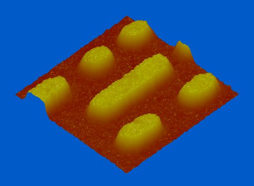
are the data marks. THe smaller bumps on and around them are
roughness features, probably grains, of nickel.
AFM images of optical disk stampers show the general shape of the data bumps, including the hegith, width, and wall slopes, as well as flaws and the fine grain structure of the Ni surface. We started working with people producing CD’s but as manufacturers develop each new generation of media, the tolerances become tighter and more critical, increasing the need for precise and accurate measurement. To assist with this, we developed the measurement software DiscTrack Plus.