- Topographic Height Imaging
- Surface Morphology Measurement: Feature size and shape
- Cross Sections and Profiles
- Measure surface polishes and finishes
- Micro and Nano Roughness
- RMS roughness (Rq)
- Mean Roughness (Ra)
- Max Height (Rmax)
- Surface Area Difference
- Rk bearing parameters
- More
- Line Edge Roughness
- Step Height
- Additional Image Modes
- Phase Imaging: Done in tapping mode, phase imaging allows mapping of material domains on the surface. Phase images are sensitive to stiffness and adhesion (stickiness) of the surface as well as edges and boundaries. Phase images can provide important information on a variety of characteristics of the sample at the micron to nanometer scale.
- Material Distributions and Chemical Domains in Polymer Blends and Copolymers
- Presence of Contaminants
- Inhomogeneity of the Sample surface
- Lateral Force/Friction Imaging: Done in contact mode, friction imaging measures the twist of the probe as it is scanned across the surface. this twist corresponds to the sideways force on the tip from factors like surface slope and coefficients of friction between the surface and the tip.
- Force Volume Imaging: While being scanned over the surface, the tip is pressed into the surface at each point and the response of the tip measured. Allows mapping of surface stiffness and adhesion.
- Techniques Involving Long Range Forces:
- Lift Mode for Measuring Long Range Forces: Most electrical and magnetic force work is done using “Lift Mode.” The tip first scans each like of the surface, then repeats the motion over that line, following the trace a preset distance above the surface. During this second trace, the response of the tip to long-range forces such as magnetic or electrical forces is measured and an image is generated based on these measurements.
- MFM: In this a magnetized or magnetically sensitive tip is used for the lift mode image. The tip reacts to magnetic forces near the sample allowing mapping of magnetic domains on the nanometer scale.
- Electrical Techniques Involving Long Range Forces:
- EFM: Similar to MFM but an electrical charge is applied to the tip. The tip then reacts to electric fields near the surface and allows them to be mapped on the nanometer scale.
- Scanning Kelvin/Surface Potential Imaging: Maps the wok function or surface potential of the surface. This technique is sensitive to many surface phenomena. Some characteristics that can be mapped include catalytic activity, doping and band-bending of semiconductors, charge trapping in dielectrics, and electrochemical differences such as those involved in many kinds of corrosion.
- Electrical Measurements in Contact with Surface
- Scanning Capacitance Microscopy (SCM): A powerful tool in studying seminconductor samples. Scanning Capacitance Microscopy allows direct measurement of activated carrier concentration on non-uniformly doped semicondutors with nanometer scale accuracy.
- Scanning Spreading Resistance Microscopy (SSRM): Another powerful tool for studying semiconductors and conductive polymers. SSRM allows mapping both topography and dopants on the surface of conductive samples.
- Conductive AFM (CAFM): Maps variations in electrical conductivity. Can be used to do things like study semiconductors, Nanotubes, Conductive Polymers, and even certain organic materials.
- Tunneling Atomic Force Microscopy (TUNA): Similar to CAFM but with much higher current sensitivity (<1 pA). Can measure conductivity through thin films and work with low conductivity samples.
- Nanoindentation and Scratching: Measure and test hardness, wear resistance on the Micro and Nano scale. The AFM presses a diamond tip into the sample surface and either withdraws, leaving an indent, or drags the tip across the surface leaving a scratch. The AFM then produces an image of the resulting indent or scratch.
- Tribology on the Nanometer Scale: The combined use of height and friction imaging, roughness measurement, and Nano-scratching and indenting allows studying the tribology of materials on the nanometer and micrometer scales.
- Phase Imaging: Done in tapping mode, phase imaging allows mapping of material domains on the surface. Phase images are sensitive to stiffness and adhesion (stickiness) of the surface as well as edges and boundaries. Phase images can provide important information on a variety of characteristics of the sample at the micron to nanometer scale.
- We can apply these analysis techniques to a variety of materials including:
- Semiconductors
- Silicon
- GaAs
- Epitaxial Wafers
- Ceramics
- Glass Fibers
- Metals & Alloys
- Composites
- Nanoscale Arrays
- Polymers
- Plastic Structures
- Biomaterials
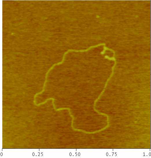
- Images of Collagen Fibers, Collagen Monomers, DNA and other rod or string-like molecules
- Paper
- Wood Pulp
- Magnetic Materials
- Electronic Materials
- Photonic Materials
- Thin Films
- Soft Coatings
- Semiconductors
- And these processes can be used to treat the results of numerous processes including:
- Cleaning
- Coating
- Corrosion
- Cracking
- Etching
- Extrusion
- Microlithography
- Molding
- Nanolithography
- Optical Disk Mastering
- Track Pitch Measurements on optical discs (CD, DVD, HD-DVD, Blu-Ray, etc.)
- Feature Size, Shape, and Position Measurements in Optical Disks
- Optical Disk Replication
- Optical Grating Fabrication
- Plating
- Polishing
- Polymerization
- Purification
- Rolling
- Texturizing
Scanning Probe Microscopy for Materials Analysis in Industry
The Scanning Tunneling Microscope originally gained attention as a simple device for imaging atoms. From that exotic beginning, there has grown a family of Scanning Probe Microscopes, of which the Atomic Force Microscope (AFM) is the most common. Various versions of these instruments operate in air, in liquid, and in vacuum. They record 3-dimensional topography, magnetic and electric fields, friction, adhesion, stiffness, optical spectra, and more.
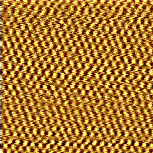
highly ordered pyrolitic graphite (HOPG).
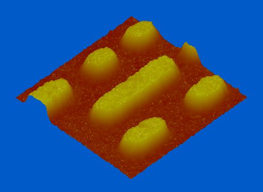
are the data marks. THe smaller bumps on and around them are
roughness features, probably grains, of nickel.
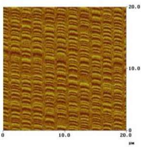
image of data on a magnetic hard disk.
Composite surfaces of industrial interest may be created either deliberately (examples include: microfabrication of thin-film recording heads and polymer processing) or accidentally (contaminants on or defects in the surface). TappingModeTM/Phase images can map the material domains with spatial resolution down to 10 nm. Such images can be a powerful aid in process control.
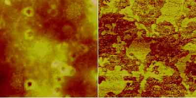
Phase images show the mechanical phase of the tapping tip relative to the drive signal which oscillates the cantilever. The phase image supplements the ordinary height image and often provides unique contrast related to material differences in stiffness and adhesion.
Nano-indentation and Nano-scratching have been developed to provide further information about stiffness and wear resistence with high sensitivity and spatial resolution.
In addition, with proper calibration specimens and our calibration correction software, standard, general use, AFM’s can make accurate and highly precise measurements.
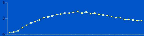
of calibration specimen without calibration
correction.
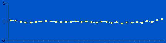
specimen with calibration correction.