Very High Resolution Calibration Reference for AFM an SEM
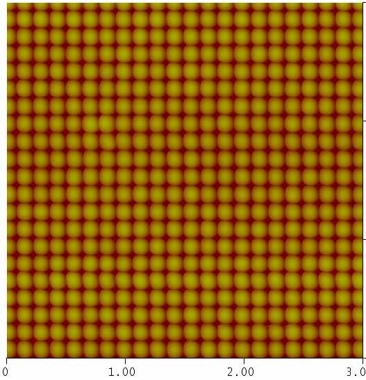
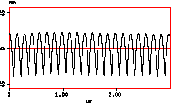
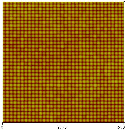
The smooth bumps produce a very regular height profile that gives improved measurement precision.
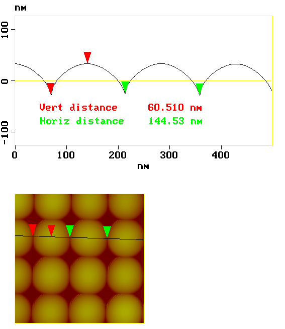
The bump height is about 90 nm. This specimen is not recommended as a height reference because it is not easy for the standard AFM probes to reach the substrate below the level between the bumps.
The above scans were made in TappingMode.
During scanning in contact mode using a 0.5 N/m SiN cantilever, we did not notice any surface or tip wear affecting the image.
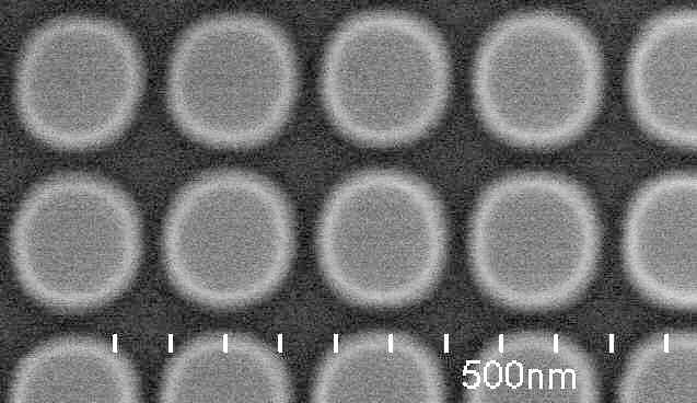
SEM Characteristics
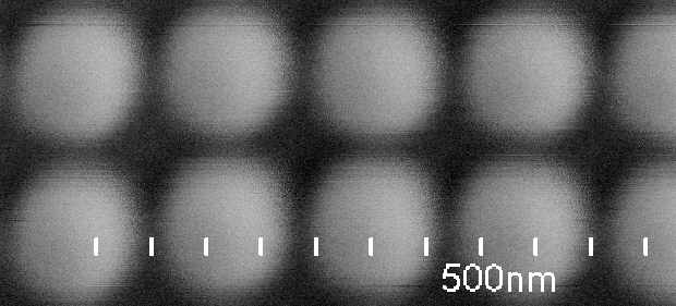
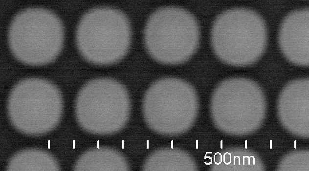
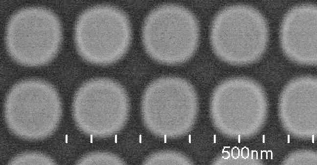
A leading independent analytical lab examined a Model 150-2D specimen in a Hitachi S4700 FE-SEM. The specimen was mounted using a conductive carbon adhesive tape and easily imaged at high resolution. Four accelerating voltages were used: 1, 5, 10, and 20 kV. No significant charging was observed at any voltage.
High magnification images
The following images were captured with a magnification setting of 100 kX. The appearance of the bumps changes with accelerating voltage as expected. At 1 kV, the electrons penetrate only a short distance, giving a surface sensitive image that shows the rounded topography of the bumps. At 5 kV, the bumps have a flat appearance. The edges appear brighter at 10 kV and at 20 kV, the edge contrast is very pronounced.
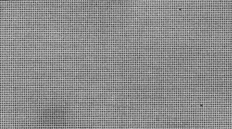
Medium Magnification
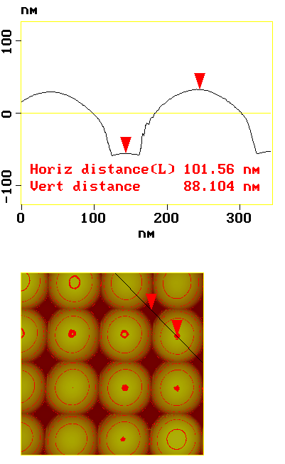
At 5 kX, the individual bumps were still well-resolved. Large fields of view show how few defects are present. The most common defects are single missing bumps or a single extra bump inserted between lattice positions. Two vacancies are present in the image shown here.
After completing the work, the analyst said: “It was nice to have something with sharp features.”