Very High Resolution Calibration Reference and Traceable Standard for AFM, STM, Auger, FIB, and SEM
General Purpose–High precision
A precision, holographic pattern providing accurate calibration in the horizontal plane for very high resolution, nanometer-scale measurements.
Period: 144 nm pitch, two-dimensional array. Accurate to +/- 1 nm. Refer to calibration certificate for actual pitch.
Surface: Etched Silicon bumps on Silicon substrate, 4×3 mm die. Bump height (about 90 nm) and width (about 75 nm) are not calibrated.
For AFM, use in contact, intermittent contact (TappingModeTM ) and other modes with image sizes from 250 nm to 10 mm. Available unmounted or mounted on 12 mm steel disks.
For SEM, this specimen works well at all accelerating voltages. Normally supplied unmounted. Can be mounted on a stub of your choice.
Usability: the calibrated pattern covers the entire chip. There is sufficient usable area to make tens of thousands of measurements without reusing any areas altered or contaminated by previous scans.
Model 150-2D. This Calibration Reference specimen comes with a non-traceable, manufacturer’s certificate. This states the average period, based on batch measurements.
Model 150-2DUTC. This Traceable, Certified Standard is a select grade. Each standard is individually measured in comparison with a similar specimen calibrated at PTB. (PTB, Physikalisch-Technischen Bundesanstalt, is the German counterpart of NIST.) The uncertainty of single pitch values is typically +/- 1.4 nm (95% confidence interval). Multi-pitch measurements provide the usual square-root of N improvement in precision. Learn about the difference betwen a traceable calibration STANDARD and an ordinary calibration REFERENCE specimen.
Easy to use
We recommend Model 150-2D because of unique characteristics that make it especially easy to use. We have tested this using the AFM in our own lab. The pattern is durable. You can scan in contact mode, which means you can calibrate and measure faster. This is the only high resolution 2D calibration specimen we know of that has all of the following characteristics that are needed for easy use:
- 2-dimensional array for simultaneous calibration of X and Y axes
- pitch << 500 nm
- array of bumps means the image contrast is high even when the probe tip is slightly dull
- high contrast in contact mode scans
- pattern covers the entire die so that you don’t have to hunt for the scan area.
AFM images
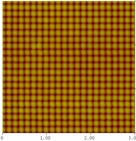
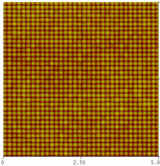
During scanning in contact mode using a 0.5 N/m SiN cantilever, we did not notice any surface or tip wear affecting the image.