Help for roughness and surface finish problems.
Surface roughness is an important indicator of product quality for many industries.
- In semiconductor manufacturing, roughness of bare Silicon wafers is measured after polishing and cleaning. Excessive roughness destroys the integrity of very thin layers, such as gate or tunnel oxide. Roughness is equally important for other electronic materials, such as SiC (silicon carbide), GaAs (gallium arsenide), and GaN (gallium nitride).
- In optics, surface roughness causes light scattering, which can be good or bad for the product, depending on the application. For high quality X-ray mirrors, both the substrate roughness and the coating roughness are measured and must be minimized. For diffusers, controlled roughness is important to achieve the desired effect; part of the control relates to the roughness power spectrum, so that the diffuse scattering is isotropic and achromatic.
- In the paper industry, surface roughness and porosity are critical factors in determining whether a paper can sell for $1/sheet (photo quality inkjet paper), $0.005/sheet (multipurpose photocopier paper), or somewhere in the middle.
- In general, the AFM demonstrates subtle, yet important, effects of surface treatment, corrosion and aging in a wide variety of materials, including metals, ceramics, glasses, semiconductors and polymers.
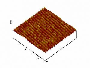
The AFM can measure surface roughness over a very wide dynamic range: from Ra = 0.03 nm to 500 nm. The combination of 3-dimensional visualization with quantitative measurement is powerful.
Also: go beyond surface roughness with Rk parameters
We can help you control surface roughness to make your products better