High Resolution Calibration Reference and Traceable Standard for AFM
For General Purpose and Metrology Microscopes
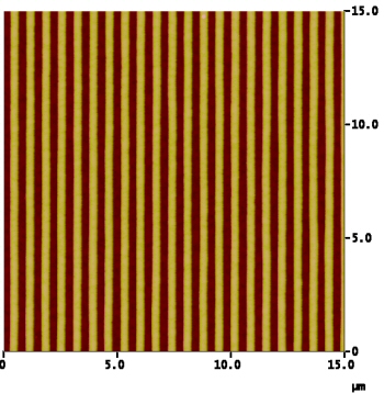
A precision pattern providing accurate calibration in the horizontal plane for very high resolution, nanometer-scale measurements.
Period: 700 nm pitch, one-dimensional array. Refer to calibration certificate for actual pitch.
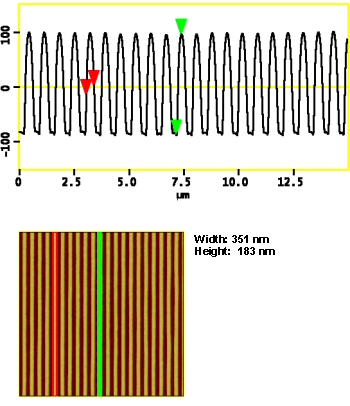
Surface: Tungsten coated developed photoresist on Silicon, 4×3 mm die. Ridge height (about 180 nm) and width (about 350 nm) are not calibrated. The specimens are produced by a series of process steps including interferometric lithography. The period of the line-space pattern is uniform without stitching errors.
For AFM, use in contact, intermittent contact (TappingModeTM ) and other modes with image sizes from 1 to 30 µm. Available unmounted or mounted on steel disks.
Usability: the calibrated pattern covers the entire die area. There is sufficient usable area to make thousands of measurements without reusing any areas altered or contaminated by previous scans. For the most accurate results, always measure pitch in an area that has uniform contrast. Do not bridge across areas with noticeably different appearance.
Model 700-1D. This Calibration Reference specimen comes with a non-traceable, manufacturer’s certificate. This states the average period (accurate to +/- 0.25 nm), based on batch measurements.
Model 700-1DUTC. This Traceable, Certified Standard is “NIST-traceable” (traceable to the SI international standard meter) by measurements made in comparison with a standard calibrated at NIST or another comparable National Lab. The uncertainty of the average and single pitch values are typically better than +/- 0.05 and +/- 0.5 nm, respectively (95% confidence interval). See certificate of traceable calibration for details. Learn about the difference betwen a traceable calibration STANDARD and an ordinary calibration REFERENCE specimen.
AFM TappingMode Scan and Average Height Profile
Easy to find patterned area
The entire surface area of the die is patterned. Defects that affect pattern period are small and easy to spot.
Appearance Issues:
Model 700-1D and 700-1DUTC specimens may have dark streaks and bright oval/round spots as shown below (oval spot):
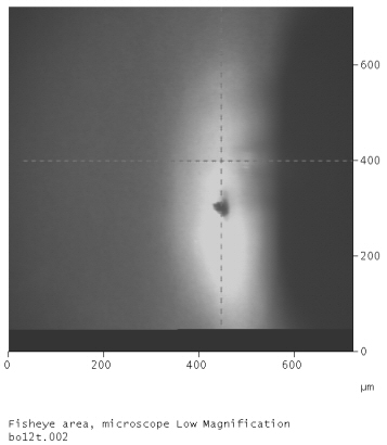
We have investigated these dark regions using AFM (atomic force microscopy) and have made the following observations:
- There is no noticeable difference in ridge height or grating pitch between the dark streaks and the normal area. – Oval/round spots generally have a small defect at the center.
- Except at the actual location of this point defect, there is no noticeable difference in ridge height or grating pitch between the track normal area and the oval/round spot.
As a result of these observations, we conclude that the round/oval spots and dark stripes sometimes seen in these specimens are cosmetic in nature and do not impede their proper use as calibration specimens if ordinary care is taken by the operator in making the calibration measurements.