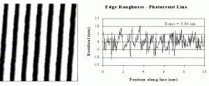
Just as the AFM can sense surface roughness, so can it sense edge roughness. Whereas surface roughness is the vertical deviation of the real surface from an ideal form, edge roughness is the horizontal deviation of a feature boundary from its ideal form. In the semiconductor industry, the narrowest lines are now less than 25 nm wide (per International Technology Roadmap for Semiconductors). The edge roughness of the polymer photoresist used to pattern those lines must be considered, since this could limit the precision of width and overlay (placement) control. We illustrate this concept using AFM scans of a photoresist pattern having pitch less than 300 nm and line width less than 150 nm. The left hand side of the figure is a 2 micron height image. The edge roughness is plainly visible, since the boundaries of the lines are slightly ragged. In order to get longer scan data, we analyzed a 10 micron image (not shown). Edge positions at 95% of the ridge height were determined on each scan line using ASM’s DiscTrack Plus™ software. We graphed edge position as a function of distance along a given line and fit the resulting curve to a polynomial. The residuals of the fit form the roughness profile, which is shown in the right hand side of the image. Here, for photoresist patterned by non-contact optical exposure, we found the rms edge roughness was 4.0 nm. For comparison, we examined polycarbonate formed by high speed injection-compression molding. The specific structure is the pre-formed groove on a recordable compact disc (CD-R). In this case, we found rms edge roughness of 6.7 nm.