Very High Resolution Calibration Reference and Traceable Standard for AFM, SEM, Auger, and FIB
For General Purpose and Metrology Microscopes
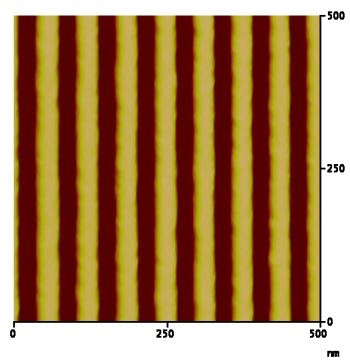
A precision pattern providing accurate calibration in the horizontal plane for very high resolution, nanometer-scale measurements.
Period: 70 nm pitch, one-dimensional array. Refer to calibration certificate for actual pitch.
Surface: Silicon Oxide ridges on Silicon, 4×3 mm die. Ridge height (about 35 nm) and width (about 35 nm) are not calibrated. The specimens are produced by a series of process steps including interferometric lithography. The period of the line-space pattern is uniform without stitching errors.
For AFM, use in contact, intermittent contact (TappingModeTM ) and other modes with image sizes from 100 to 3000 nm. Available unmounted or mounted on steel disks.
For SEM, this specimen works well at a wide range of accelerating voltages (1 kV to 20 kV have been tested) and calibrates images from 25 kX to 1000 kX. Normally supplied unmounted. Can be mounted on a stub of your choice.
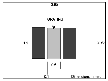
Usability: the calibrated pattern covers a 1.2×0.5 mm area. There is sufficient usable area to make thousands of measurements without reusing any areas altered or contaminated by previous scans. For the most accurate results, always measure pitch in an area that has uniform contrast. Do not bridge across areas with noticeably different appearance.
Model 70-1D. This Calibration Reference specimen comes with a non-traceable, manufacturer’s certificate. This states the average period (accurate to +/- 0.25 nm), based on batch measurements.
Model 70-1DUTC. This Traceable, Certified Standard is “NIST-traceable” (traceable to the SI international standard meter) by measurements made in comparison with a standard calibrated at NIST. The uncertainty of the average and single pitch values are typically better than +/- 0.05 and +/- 0.5 nm, respectively (95% confidence interval). See certificate of traceable calibration for details. This 70-nm pitch standard was the subject of a recent interlaboratory comparison involving ASM, NIST and NMC/A-STAR (the Singapore counterpart of NIST). See our publications.
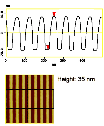 The ridge height is about 35 nm. This specimen is not recommended as a height reference because the standard AFM probes may not always reach the substrate level between the ridges. Nevertheless, image contrast is high, even when the tip is slightly dull. You can scan in contact mode, which means you can calibration and measure faster.
Easy to find patterned area
The patterned area is easy to find. The three rectangles shown in the sketch below are visible in reflected light, with either the unaided eye or an optical microscope. In a low magnification SEM image, the contrast is reversed. The central rectangle, which is the grating pattern, is relatively bright. The grating lines are parallel to the long side of the rectangle, as suggested by the high magnification SEM image.
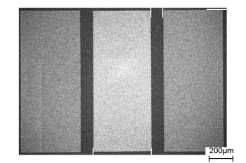
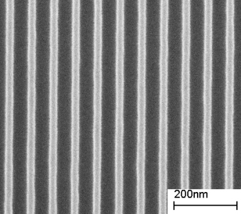
Magnification = 200 kX
Voltage = 5 kV
See also Model 70-1DUTC – Questions and Answers.
Price and ordering information.