AFM in the Telecommunications Industry
Atomic Force Microscopy has many applications in the telecommunications industry.
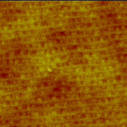
Semiconductors
Data processing is a big part of telecommunications. New semiconductors that are faster with smaller gates and narrower traces push the limits of manufacturing technology. Atomic Force Microscopy provides an in-depth look at the surface structures of electronic materials such as semiconductor wafers.
Fiber Optics
Fiber optics is a prime method of high-speed communications. Surface irregularities in the fibers are sources of signal loss. These irregularities can also form stress points leading to mechanical failure of the fiber. Atomic Force Microscopy, by producing a true three-dimensional map of the surface, allows developers and manufacturers to examine the surface structure of fibers on the micron and nanometer scale providing information to help improve the efficiency and durability of fibers.
Structural Materials
Polymers, metals, and composites: whether it’s cable cladding, relay tower structures, or satellites in orbit, components and structures used in telecommunications often face very harsh environments. Understanding the surface structure and composition of these structures provides important insight into making materials that can endure these environments for increased system life and lower life-cycle costs.
These are just a few of the applications of Atomic Force Microscopy in the Telecommunications industry. Contact us to see how we can help you.